
Technology transfer · Licensing · Acquisition opportunity
Planar Optical Light Guides for Light Collection and Collimation
Background
Planar optical light guides are making a rapid entry into many light management and energy applications. With the advent of low-cost optical materials and microreplication technologies, edge-lit light guides became commonplace in smartphones, computers and TV displays and are now being tried for general lighting and solar energy.
In edge-lit LED illumination devices and LCD displays, the angular distribution of the light beam emitted by a light guiding panel (LGP) is defined by the technology used to extract light from the light guiding panel (LGP). The conventional features such as microgrooves or white paint dots distributed over the surface area can provide good brightness uniformity but lack the ability to form a directional light beam. Achieving high collimation and custom angular patterns is particularly challenging.
In solar energy applications, lightguides can condense sunlight to a high degree similarly to concentrating mirrors or lenses while also providing the benefit of a thin form factor. For example, the direct sunlight can be collected by a large surface area of the LGP and focused onto its edge where it can be converted into electricity by a small solar cell or into heat by a thermal absorber. However, such devices require solving the problems of efficiently injecting light into the LGP and delivering the injected light to a prescribed location.
Description
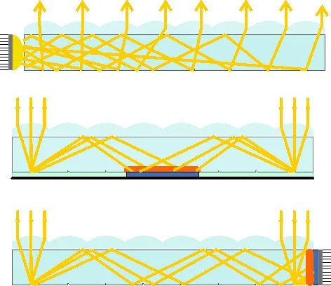
Researchers at Lucent Optics have invented a new type of light guiding plates and films that can efficiently collect and distribute light beyond the limits of conventional designs. The new light guide includes specially designed optical microstructures that provide unprecedented control over light coupling and extraction.
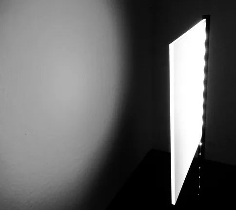
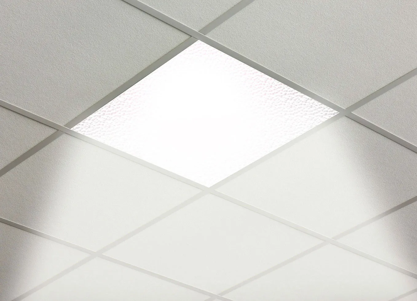
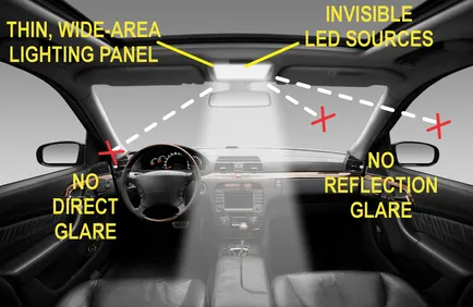
In light emitting applications, such microstructures can be designed to precisely shape the light beam to any prescribed spread angle with a soft or sharp intensity cutoff. Narrowing the emitted beam allows for significantly increasing the apparent brightness of LCD displays, illumination efficiency of LED lighting fixtures and eliminating the energy waste.
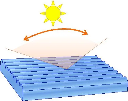
In light collecting applications, the microstructures can be designed to capture nearly all of the incident light rays and direct them to an edge or any other location of the light guiding plate or film with minimum losses. This can especially benefit solar energy applications requiring high sunlight concentrations and compact form factors. The light guides can be designed with a linear or two-dimensional pattern of the microstructures and can be made from common glass or optical plastic materials.

Applications
- LED lighting panels
- Edge-lit LED signs and LCD displays
- Solar concentrators
- Optical sensors and waveguides
- Photonics
Advantages
- High optical efficiency
- Ultimate control of beam angle and brightness uniformity
- Compact form