DISRUPTIVE SOLAR ENERGY & LIGHTING INNOVATIONS  

OPTICAL ENHANCEMENT FOR PHOTOVOLTAIC MODULES

BACKGROUND: WHY LIGHT TRAPPING?


The semiconductor materials used in photovoltaics are utilizing only a portion of energy available in sunlight. A significant part of solar energy spectrum is either rejected or ignored by the solar cell resulting in energy waste and limited overall efficiency.

The amount of light which remains unabsorbed varies from 15% to 50% depending on the cell design and optical properties of the material used for light capture. Recovering light which is otherwise lost is an attractive way of increasing the efficiency of PV panels and reducing the cost of solar energy.

Light trapping is about recycling the light rays that are not absorbed by the layer of a nominal thickness. When properly implemented, it increases the optical path of light rays in the photoabsorbtive material without increasing the layer thickness thus promoting a more complete absorption and eliminating energy and materials waste.


Light trapping is employed in virtually every solar module in order to enhance light capture and absorption by the cells. The effect of light trapping varies based on the type of photovoltaic materials and the overall cell design. About 90% of all modules produced today are based on crystalline Si cells each having both anti-reflective coating and special texturing on its light-receiving surface. Light trapping plays an extremely important role in maintaining the optimal efficiency aand lowering the cost of the module. For mono c-Si substrates, the most common texturing method is anisotropic chemical etching which produces random surface pyramid microstructure. The pyramids reduce the effective optical reflectivity of the surface and increase of the optical path length of captured sunlight inside the substrate. It is estimated that without surface texturing and AR coating, solar modules would be 30-50% less efficient and more expensive per peak watt.

BUILDING A BETTER LIGHT TRAP


Scientists at Lucent Optics have developed a new concept of universal light-trapping glass that will significantly improve the conversion efficiency of most types of photovoltaic modules including thin films and crystalline Si panels. The targeted product is a drop-in replacement of the conventional front glass in solar modules which will dramatically increase light absorption regardless of the cell type and will enable generating more electric current using much less photovoltaic materials.


The new solar glass is an award-winning technology which employs a specially textured surface and low-refractive-index layers that work together to trap light within the solar cell using the total internal reflection (TIR). Such light trapping allows for recycling light that remains unabsorbed by the solar cell in the first pass. The patented structure of the new solar glass increases the effective light path through the photoactive layer by up to a few hundred times and enables complete light absorption even at extremely low thicknesses of the photoactive layer. As a result, unprecedented material savings and cost reduction can be achieved in solar module manufacturing.


This approach to enhancing light absorption in solar cells is extremely efficient, covers the entire spectrum of solar cell sensitivity and far surpasses the well known 4n2 “ergodic” limit of absorption enhancement. Importantly, it eliminates the need of cell texturing and enables such cells to operate in the most optimal way. The light-trapping solar glass can even recycle light reflected by the cell’s grid fingers and bus bars thus eliminating the usually unavoidable losses related to contact grid partially blocking the sunlight from reaching the semiconductor layers.


ENHANCING ABSORPTION AND PHOTOCURRENT GENERATION

COMPARISON OF PHOTOCURRENT ENHANCEMENT USING DIFFERENT LIGHT TRAPPING APPROACHES

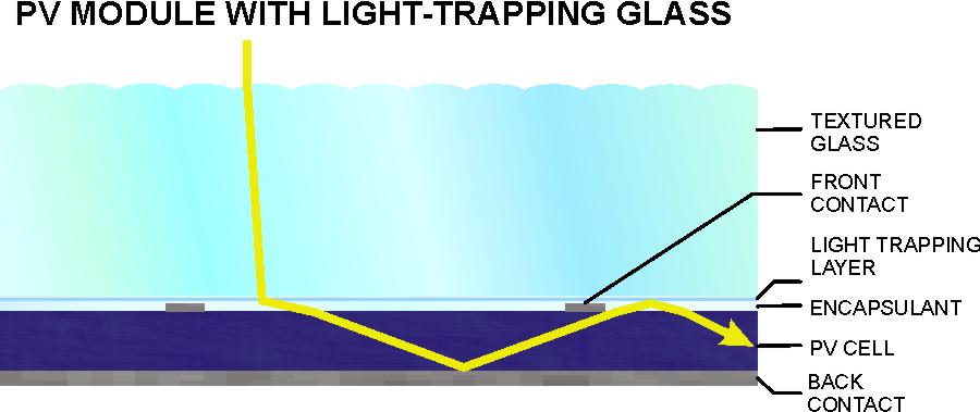
The light trapping glass operates using simple optical principles and is wavelength- and absorber- independent, which makes it compatible with all types of solar cells, including wafer-based and thin films. In addition, it can be used for both metal grid and TCO based module architectures.


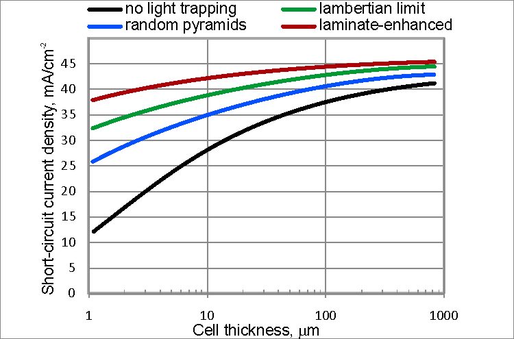
The research team of Lucent Optics has conducted proof-of-concept studies of the light trapping PV technology which included both modeling and component-level prototyping. In the “ideal” approximation, light path enhancement factors of over 1,000X were obtained. The results obtained for realistic models of the PV module with conservative design limitations have shown broad-band light path enhancements factors up to 200X compared to the bare Si wafer. Such dramatic enhancement in the light path length yields a potential of 6-7 times reduction in Si reflectance and over a hundred times improvement in light absorption in the IR spectrum.


The graph on the left shows the anticipated impact of employing the proposed technology on c-Si PV cell performance. The black line shows short circuit density versus cell thickness for a bare cell (no light trapping). The blue line corresponds to the same cell having state-of-the-art random pyramid texture. The green line indicates the theoretical limit of light trapping with substrate texturing. The red line (on top) corresponds to the case of bare wafer covered with the light trapping glass.

PV MODULE COST REDUCTION USING LIGHT-TRAPPING GLASS


There are two main strategies of reducing the module manufacturing cost using the light trapping glass/laminate technology. The first one is to increase the efficiency of the module without changing the cell technology, thus proportionally reducing the non-cell costs of the module in terms of $/W. For example, the efficiency of mono-Si modules could be achieved using 20% cheaper poly-Si cells thus providing a major breakthrough in module cost reduction without altering the overall manufacturing process. The second strategy is to significantly reduce the thickness of the photoactive layer thus saving the costs associated with expensive semiconductor materials. Using this approach, for example, the thickness of silicon wafers can be reduced from the current 180 micrometers down to 10-50 micrometers without performance penalties associated with poor light absorption in thin layers of bulk silicon, resulting in a cost reduction of up to 35%. Since the light trapping laminate is a simple replacement of the front glass, it does not alter the overall module structure. Therefore, manufacturers can exercise either one of both strategies in high-volume production and drastically reduce the PV module manufacturing cost without incurring capital costs typically associated with switching to new technologies.

OTHER LIGHT HARVESTING APPLICATIONS

The light-trapping laminate is a universal optical trap and can also be used for improving efficiency in other types of light harvesting products. In panel-type photo-bioreactors, such as those used for producing bio-fuels from algae, it can dramatically enhance light absorption, solve the common problem of non-uniform volumetric light distribution and reduce the weight of the reactor panels. In sunlight-driven water purification systems, the light trapping laminate can increase productivity and reduce system dimensions and cost. The cost of certain types of optical sensors can be reduced by employing the light trapping layer and reducing the intake of photosensitive semiconductor materials which typically represent the largest share of the sysem cost.